SMT焊接不良及图片说明5--Open Joint空焊
日期:2009-12-07 21:27 点击:619
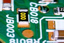
5.Open Joint( 空焊 )


拒收 良好情r
缺c描述 :
Solder does not connect pad and lead entirely.
ACCEPTABILITY
It is not consider to be a defect if the joint covered more than 50% of solder in the copper pad.
PROBABLE CAUSES
- Solder is wicked up by the lead which removed the required amount of solder to form a solder joint
- Lacked of coplanarity which result in bent lead or insufficient solder
- Grain boundary cavitation
|
- Solder sucked into vias
- Incomplete outgassing causes entractment of gases generated from evaporation and decomposition chemicals used in flux or paste
- Improper volume of solder
- Excessive intermetallic compound
|
POSSIBLE PREVENTIONS
- Optimize the heating profile so that it will be compatible with the chemical make-up of solder paste or flux
- Allow a sufficient dwell time in the molten state
- Optimize the cooling rate to balance the gas release mechanism and microstructure development
- Maintain the temperature in the soldering machine to allow formation of good solder joint
|
- Select alloy composition with high fluidity and controlled intermetallic formation
- Coplanarity should be sufficient so as not to result in either bent lead or insufficient solder
- During PCB design, avoid solder joint with an excessive large interface area with excessive thickness
- Minimize the gas generation
|
Rework
The open joint is soldered by using a chisel-shaped soldering tip placed against it long enough such that the transfer of heat is sufficient enough before placing the solderwire close to the tip of the iron.


