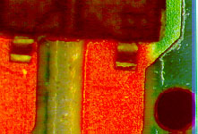
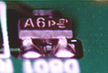
SMT焊接不良及图片说明6--Skip缺a
日期:2009-12-07 21:27 点击:600
6.Skip( 缺a )


拒收 良好情r
缺c描述 :
No solder on pad or component metallization.
PROBALBLE CAUSES
- Wave did not overcome surface tension of solder
- Surface tension of solder too high
- PCB or pallet was put under too much pressure when put into the finger conveyor or not given enough room to expand during warm-up and has bowed prior to entrance into the solder pot.
|
- Gas accumulated at joint
- Geometric orientation of components causing shadowing of joints
- Pallet warpage
- Wave not even or level
- Conveyor not parallel to solder surface
|
POSSIBLE PREVENTIONS
- Change the direction of PCB entering into the solder pot
- Dry flux properly in the preheat zone
- Check pallet and make sure it is place correctly on belt or chain
- Adjust finger pressure and groove pallet fixture to allow for expansion
|
- Adjust the wave height
- Adjust conveyor
- Use flux with lower solid contents
- Apply less flux
- Better curing of adhesive
- Drill holes in order to let gas escape
|
REWORK
The skip joint is soldered by using a chisel-shaped soldering tip placed against it long enough such that the transfer of heat is sufficient enough before placing the solderwire close to the tip of the iron.


