Wills说30%的印刷线路板问题来源于表面装贴,38%的零件问题与BGA有关。
参与者可以提前Email问题及图片到processdefectclinic@ipc.org. 注册在线免费讨论会议请访问:www.ipc.org/defects-registration, 并且请与当地时间访问:www.worldtimeserver.com
BANNOCKBURN, Ill., USA, November 30, 2010 — With hundreds of opportunities for problems to surface during the electronics manufacturing process, it is a credit to the manufacturing and engineering talent of the industry that planes fly, pacemakers keep hearts beating and phones are at the ready to provide Facebook updates or even make a call. To keep these dedicated professionals up-to-date on the latest causes and cures for assembly and solder defects, IPC and the U.K. National Physical Laboratory (NPL) have teamed up to sponsor a free webinar at 12:00 pm (noon) U.S. Central time on January 27, 2011 — a precursor to the hands-on, three-day Process Defects Clinic that will be held at IPC APEX EXPO in April.
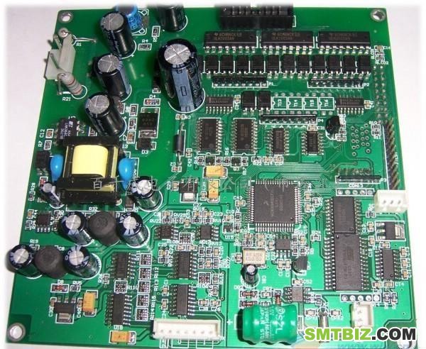
According to Bob Willis, NPL process defects database consultant, the advent of lead-free technology made every step of the assembly process more difficult. “Common process problems today relate to the correct selection of printed board materials, surface finishes and soldering materials,” says Willis. “While some defects are cosmetic, others have significant reliability implications. Companies incur a great deal of cost if they can’t distinguish between the different types.” Willis estimates that 30 percent of printed board defects relate to surface finishes and 38 percent of component problems are related to ball grid arrays. Queries about BGAs top the searches in the NPL database.
During the webinar, Willis will share common problems, helpful solutions and ways to investigate the root causes. The webinar will cover the most frequent defect types; how to monitor process defect levels, record defects for investigation, and coordinate process parameters; the most common wave, selective and reflow soldering defects; and how to find defect causes and cures.
Participants can e-mail their problems and photos in advance of the webinar for discussion and resolution to processdefectclinic@ipc.org. To sign up for the free webinar, visit www.ipc.org/defects-registration. To calculate the time in your area, visit www.worldtimeserver.com and use United States/Illinois time at 12:00 pm for comparison.
In April, Willis will staff a free process defects clinic at IPC APEX EXPO, taking place at the Mandalay Bay Resort & Convention Center in Las Vegas. Over three days, April 12–14, 2011, the clinic in booth 217 will help identify process problems for visitors and provide suggested solutions. Attendees of the event are invited to bring electronic assemblies for examination or process problems for discussion. Pre-register for free exhibit hall admission to IPC APEX EXPO and the on-site process defects clinic at www.ipcapexexpo.org/register.


